


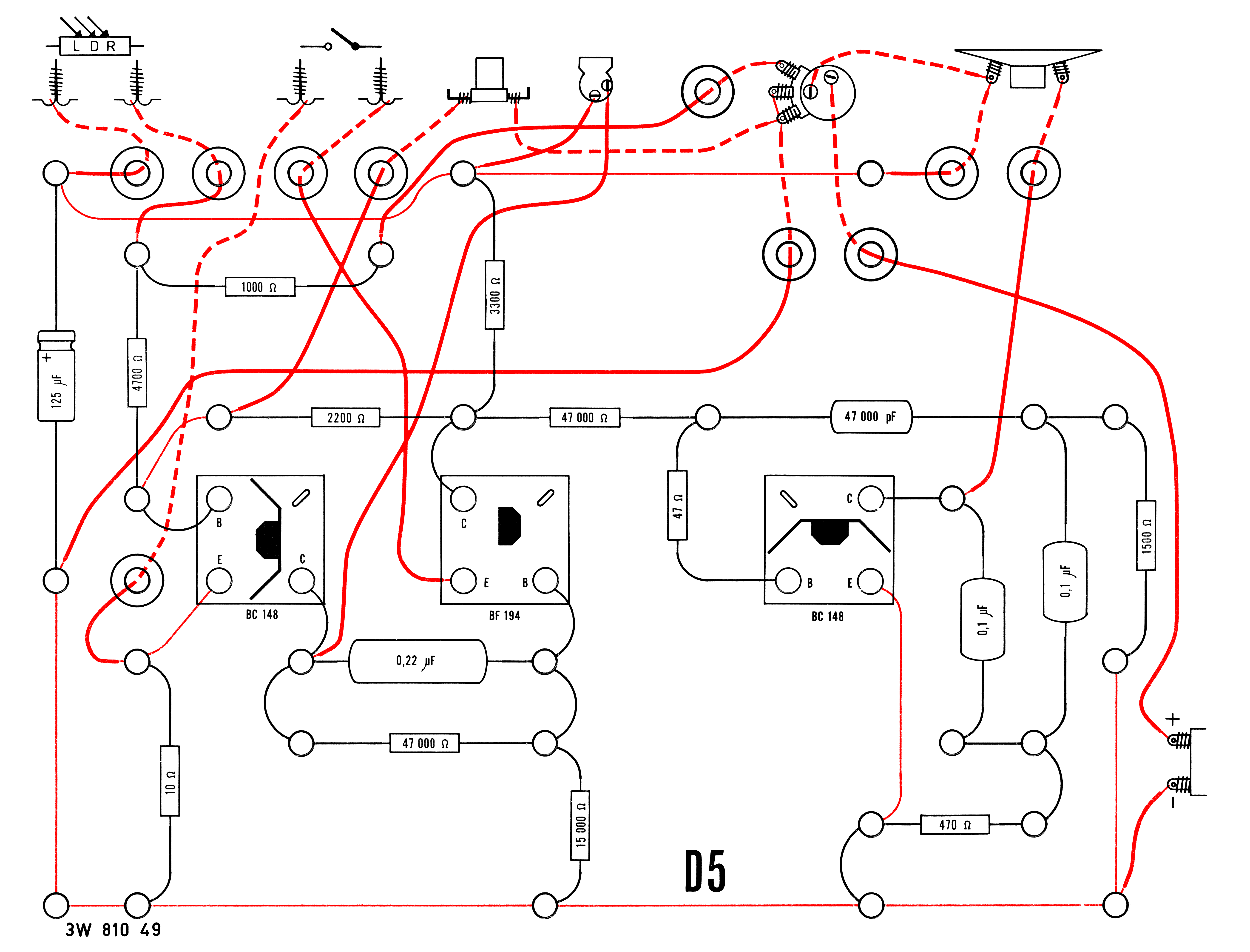
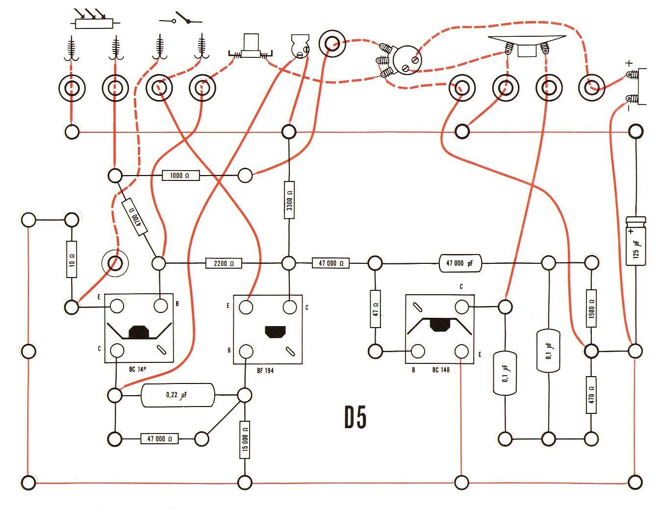
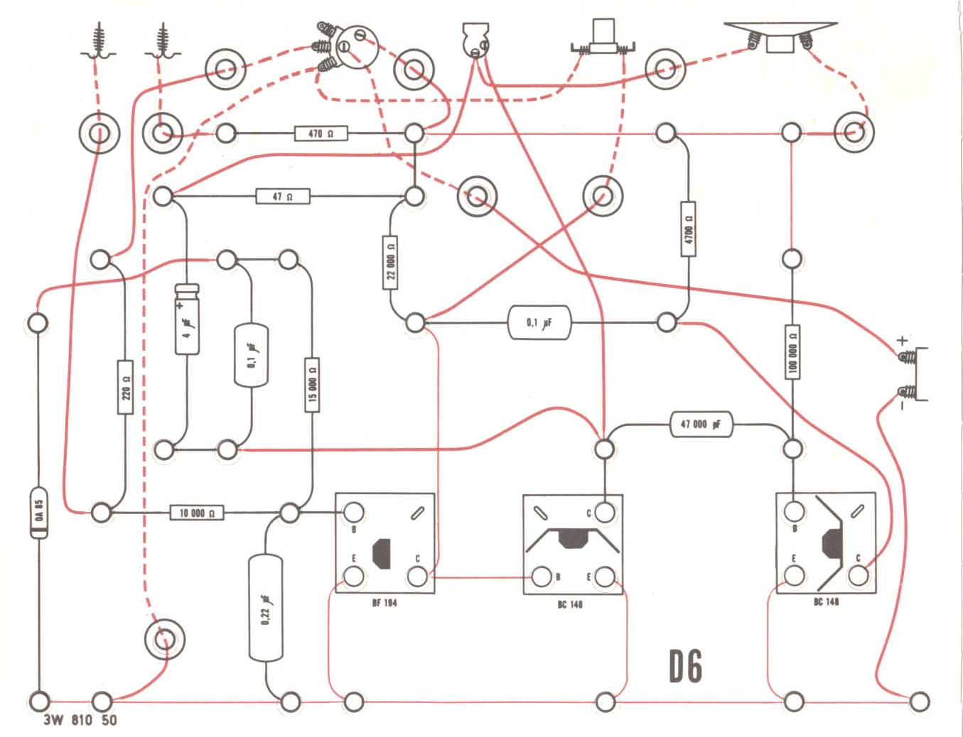

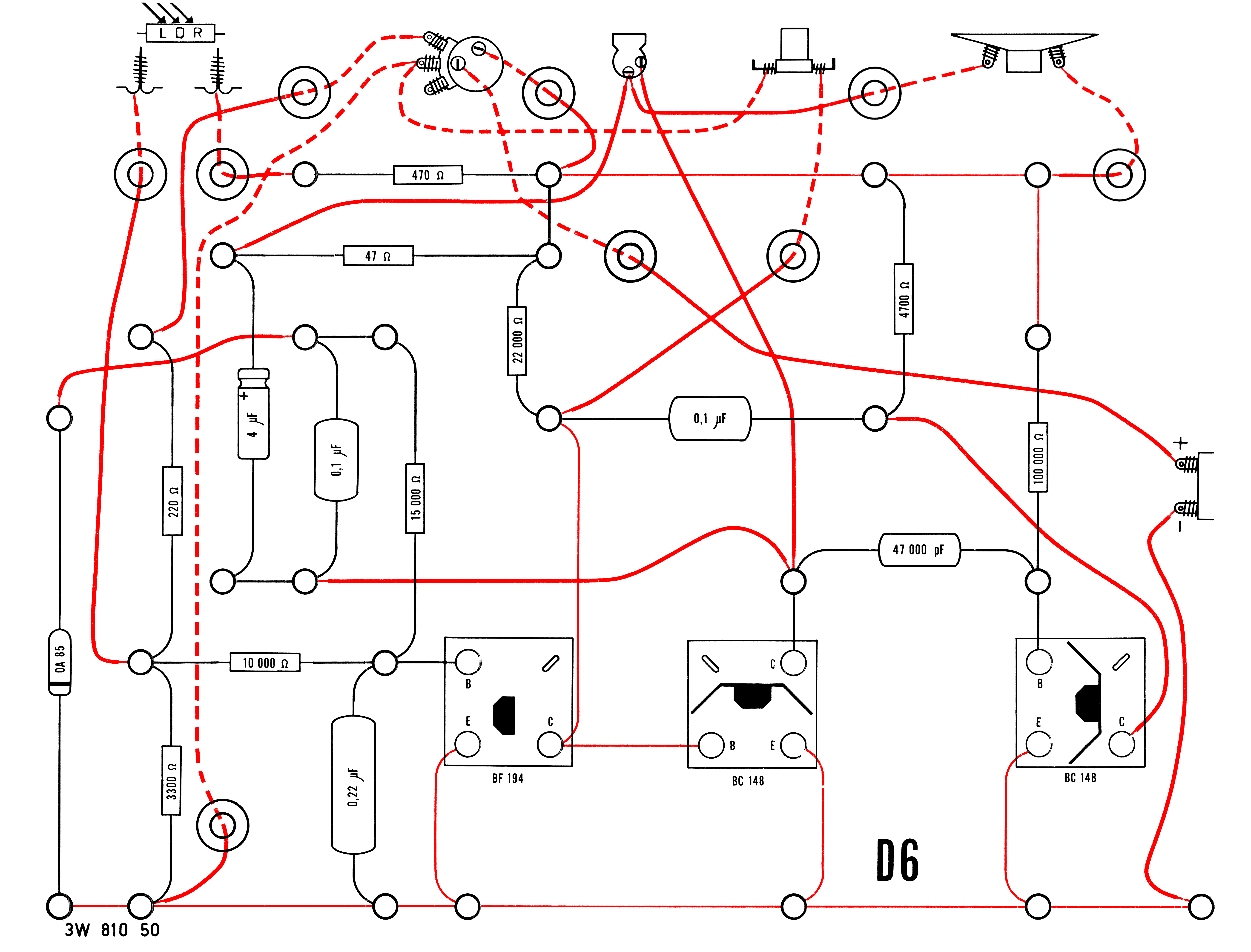


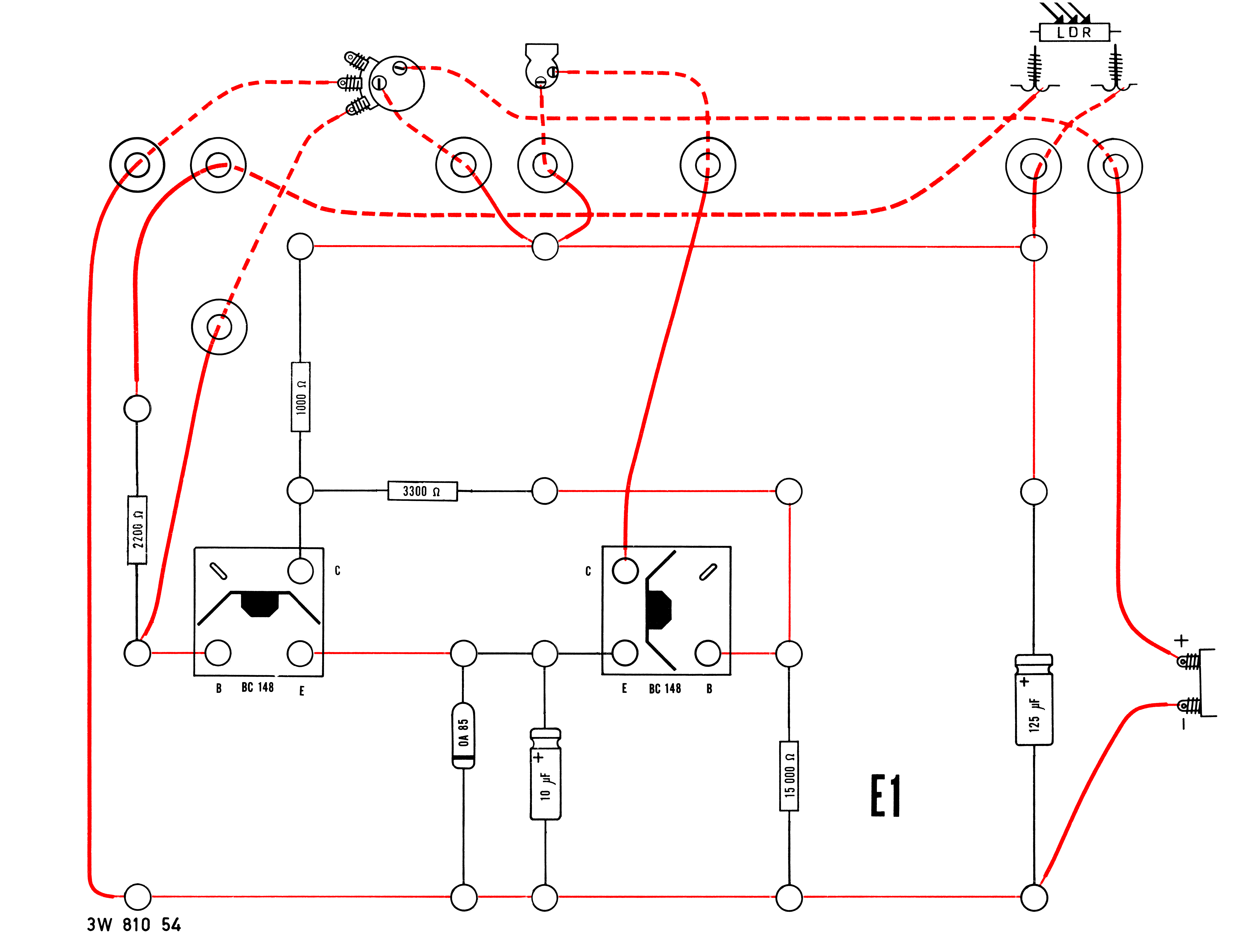
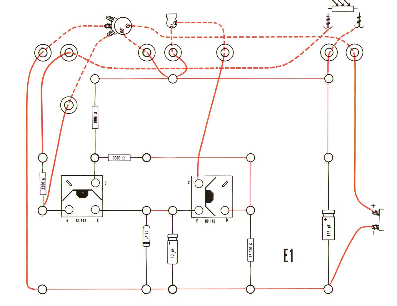
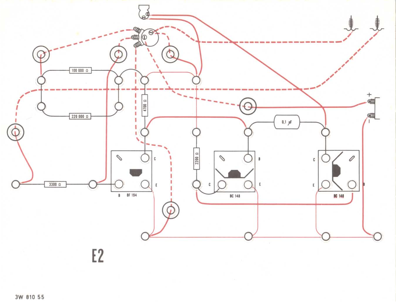
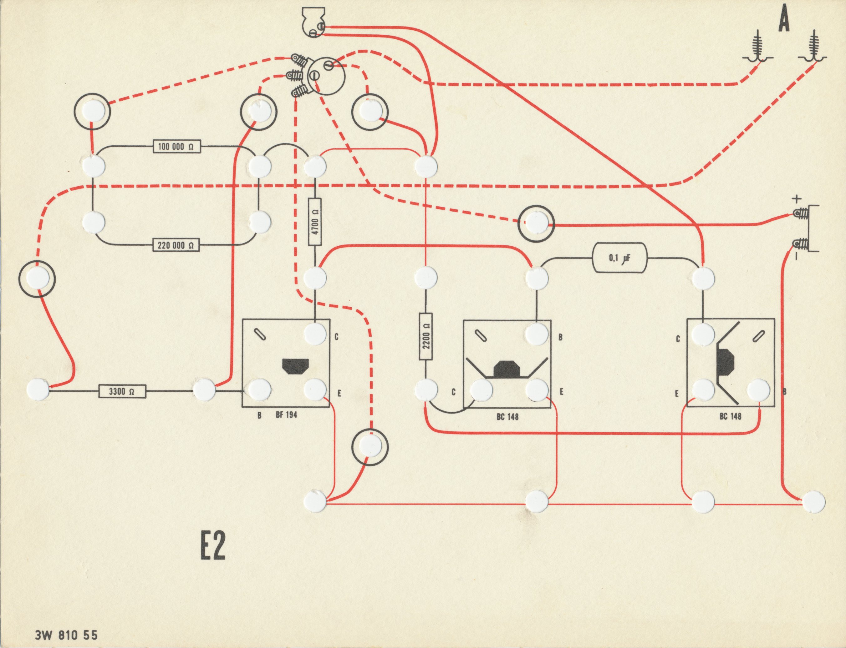

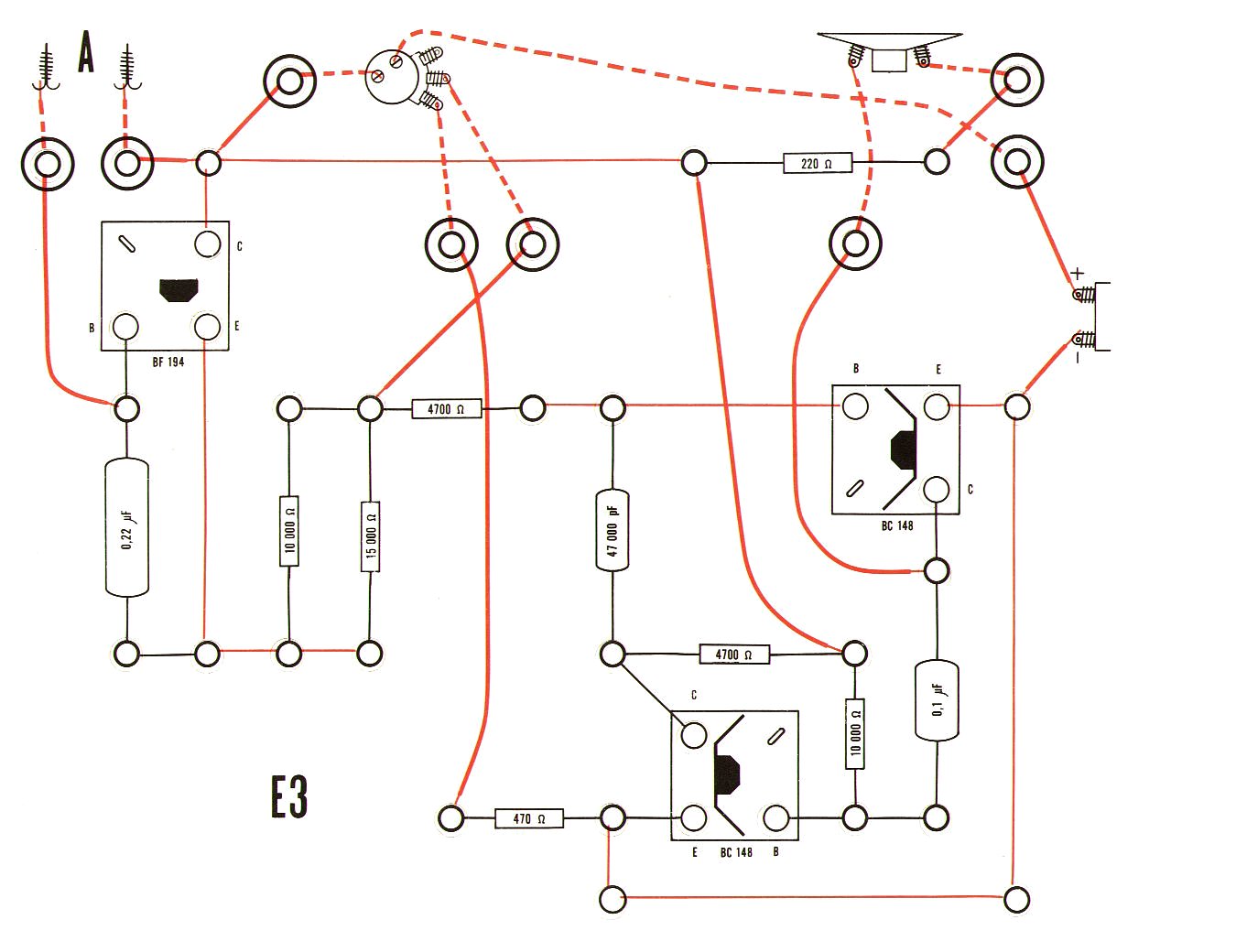
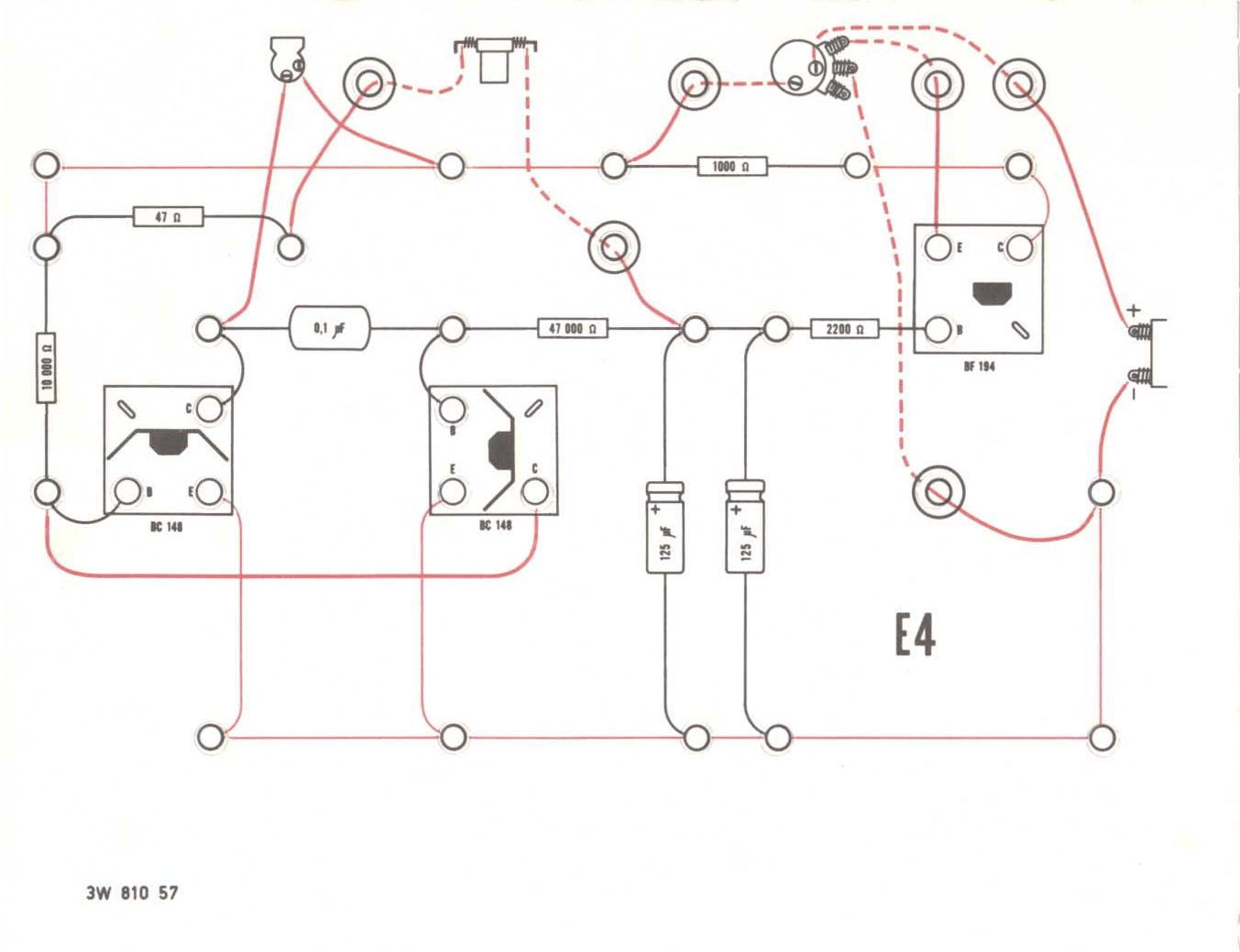
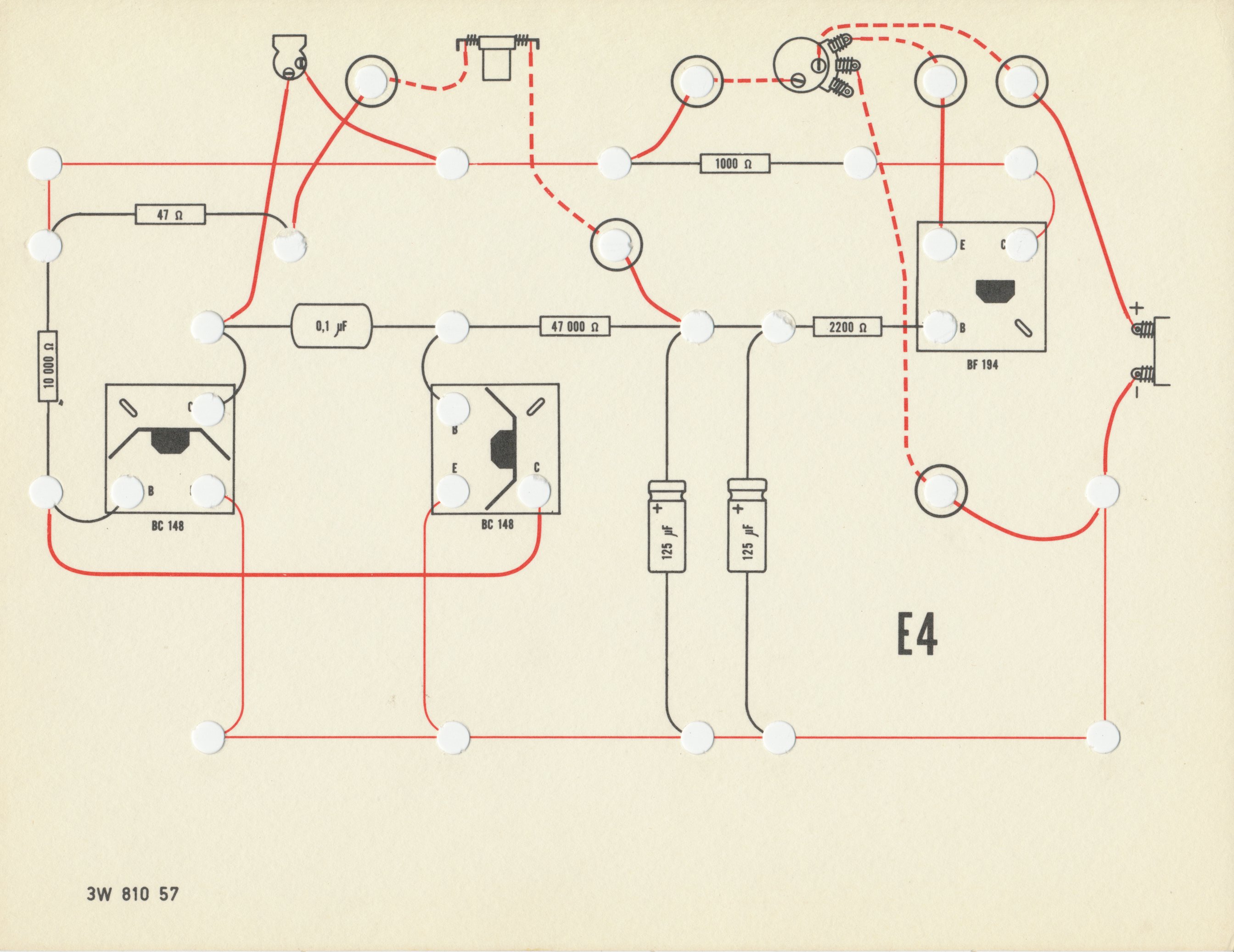
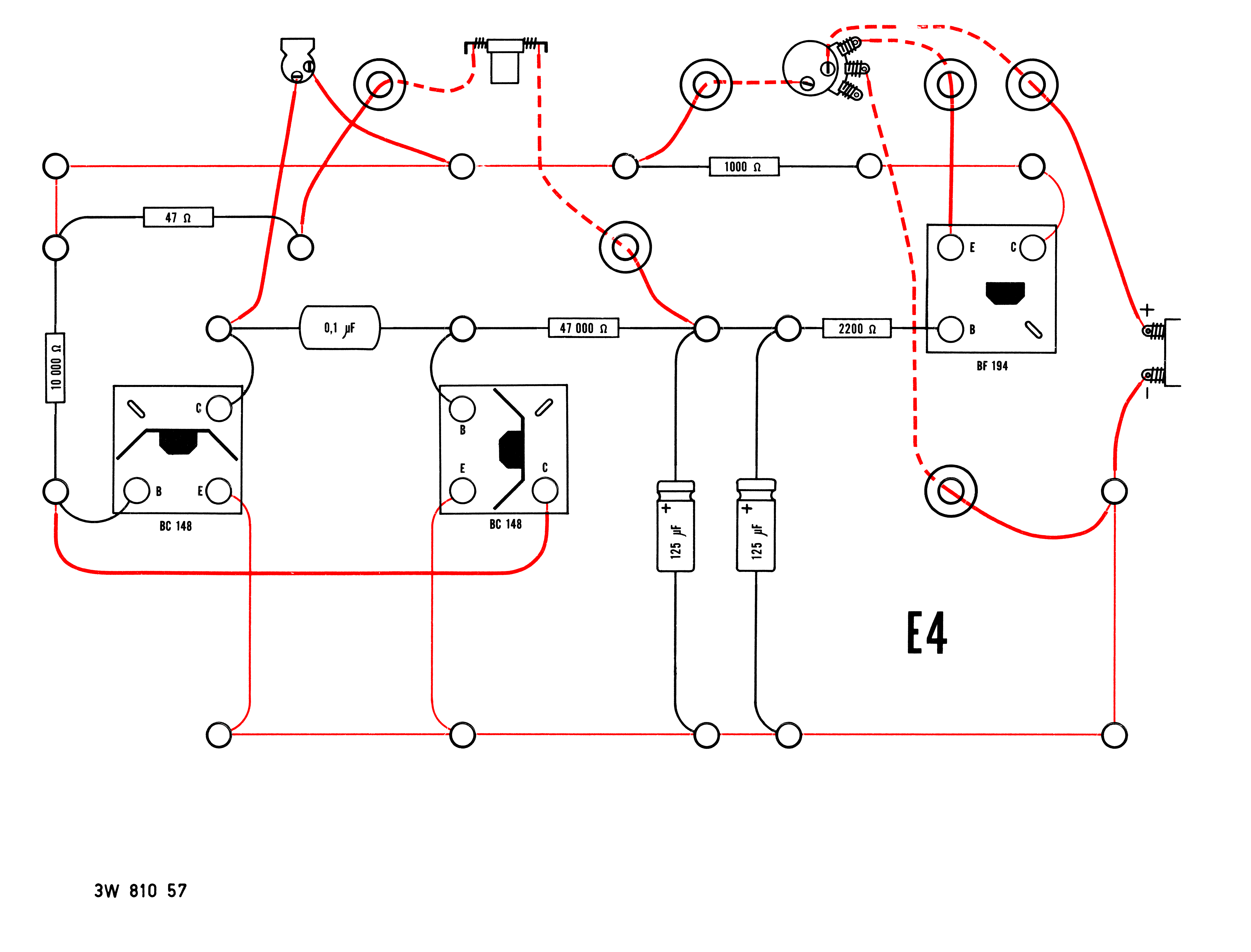


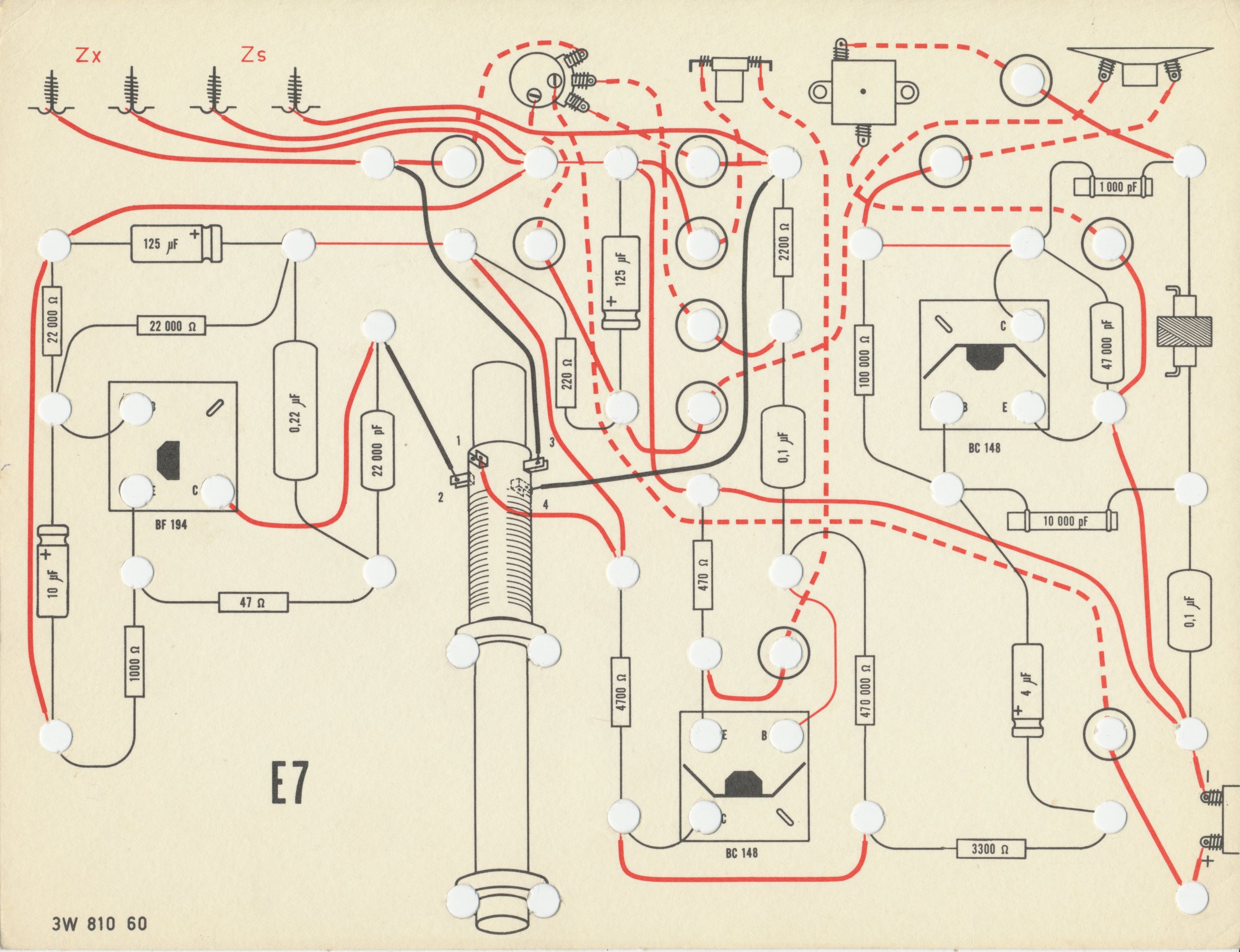
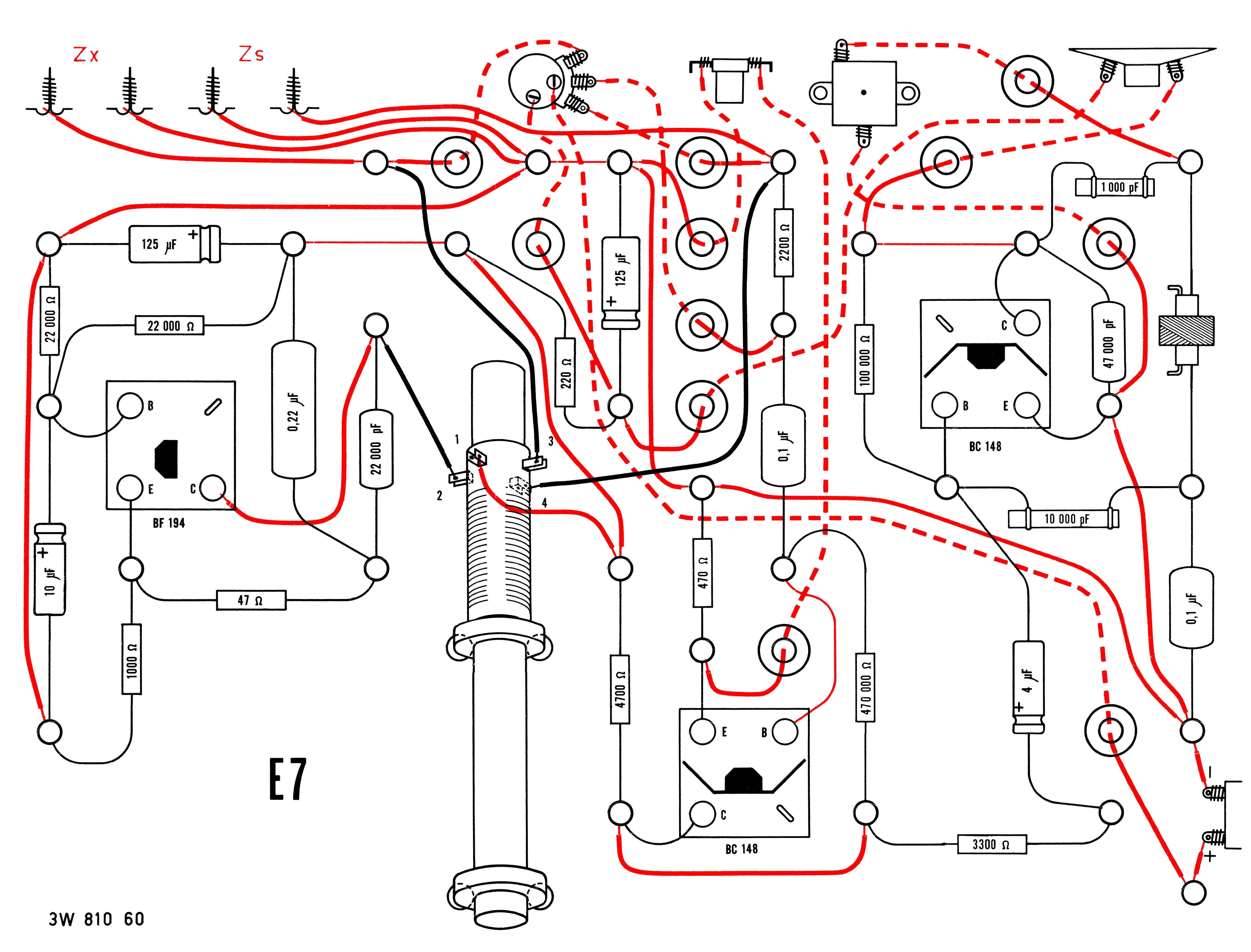
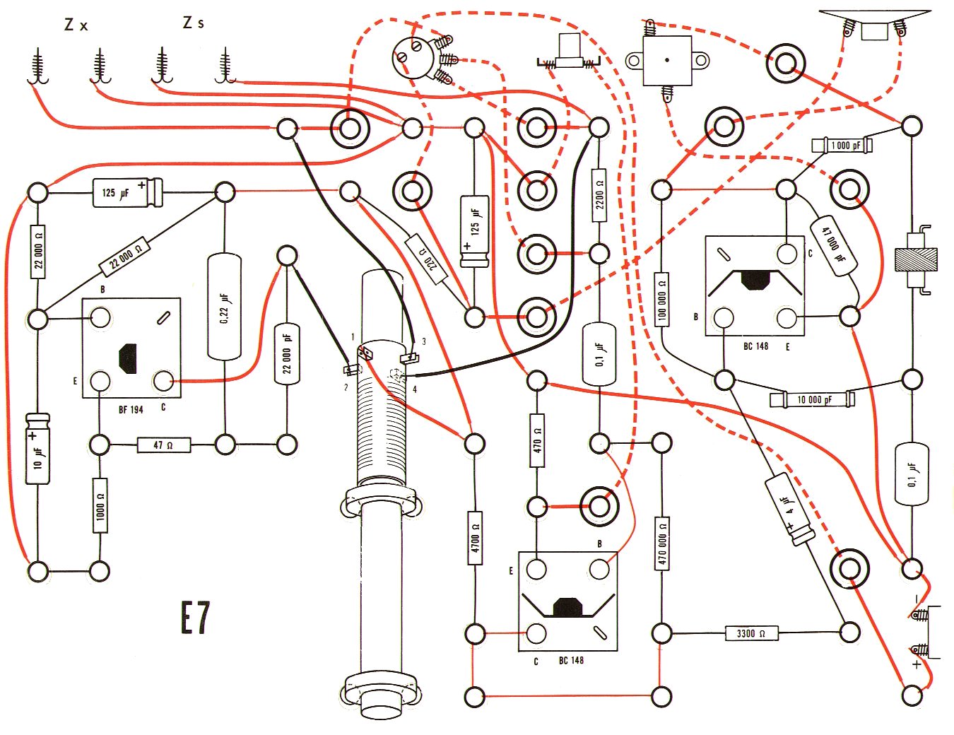
Like most other aspects of the long-lived kits, the construction diagrams of EE 1003 exist in different versions; in this case at least four. The diagrams are generally not dated, but two of the sets have printing codes indicating that they are the third and fourth versions, and the remaining two are older than these.
| Version 1 | Version 2 Minor revision mainly adding icons to front panel connections. | Version 3 Minor revision; different front panel icons | Version 4 Major revision, straightening many wires |
|---|---|---|---|
|
|
|
|
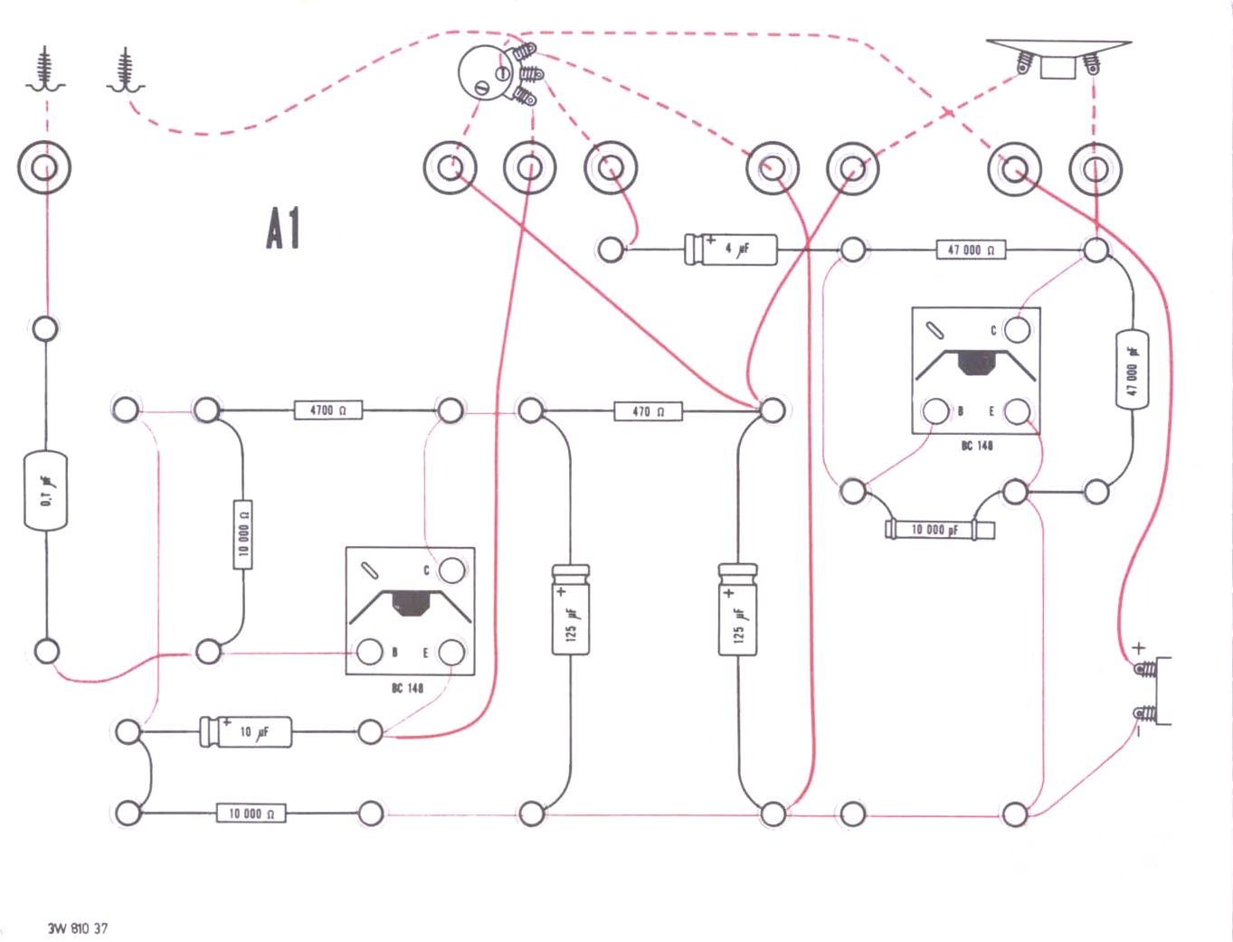
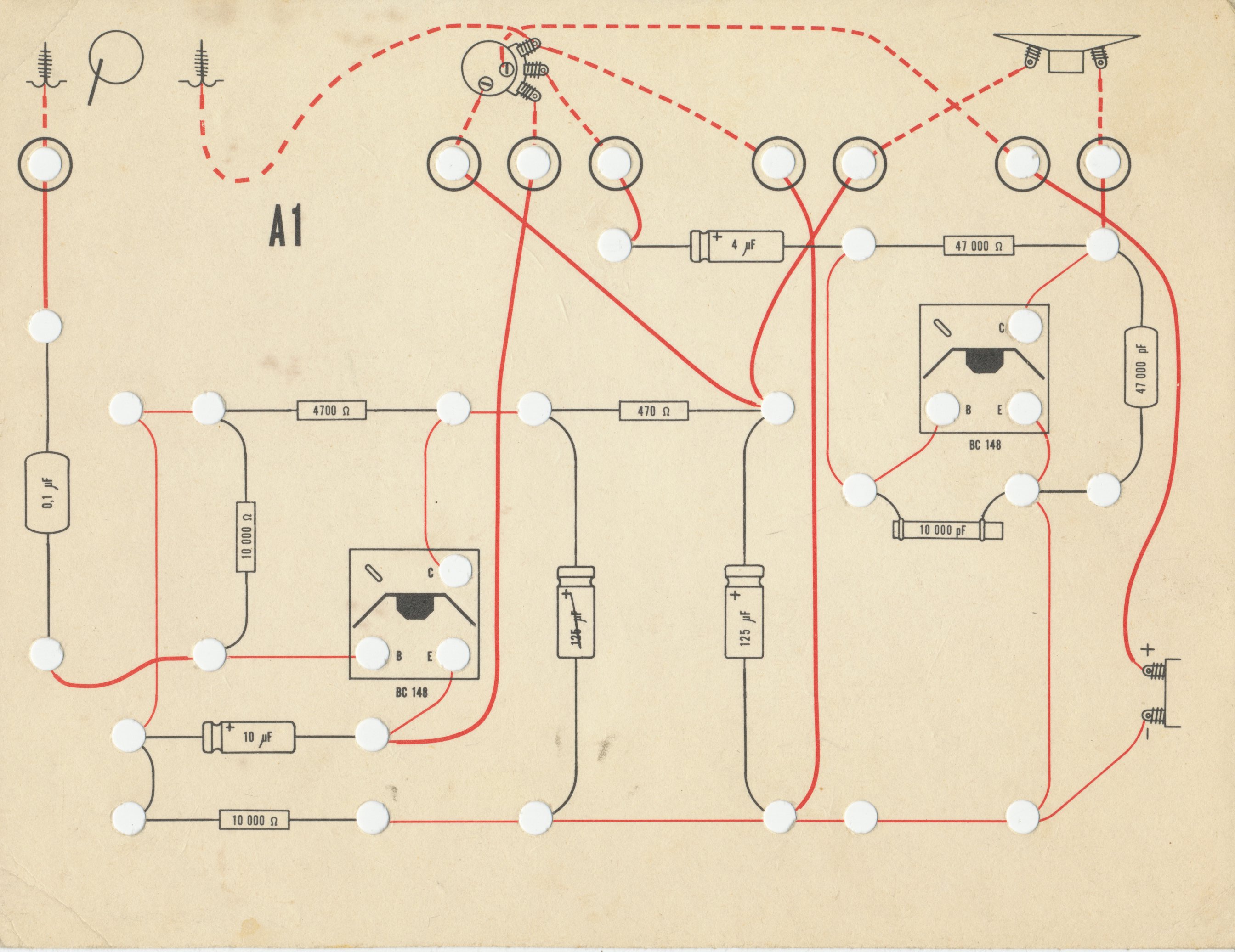
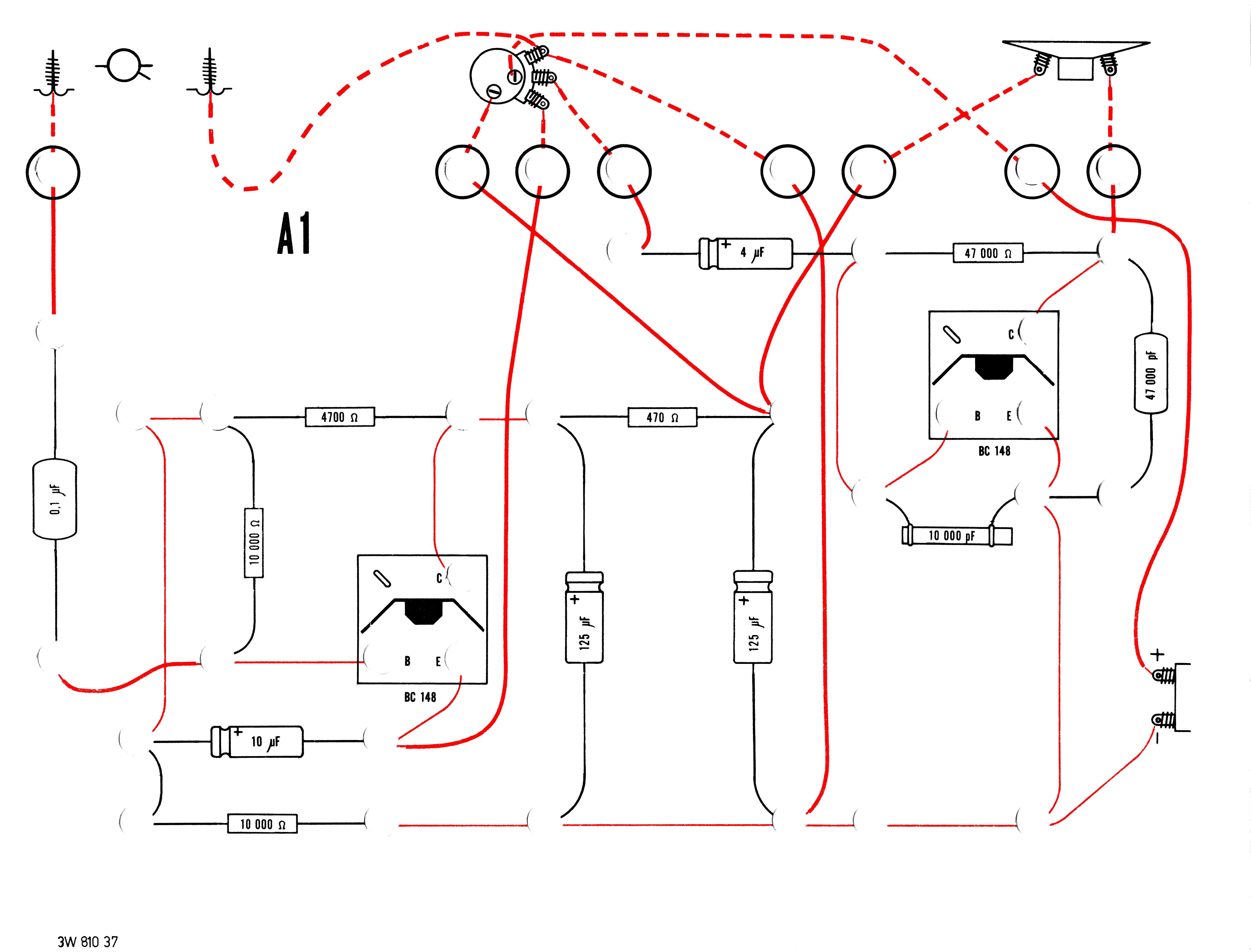
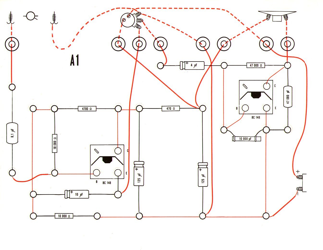
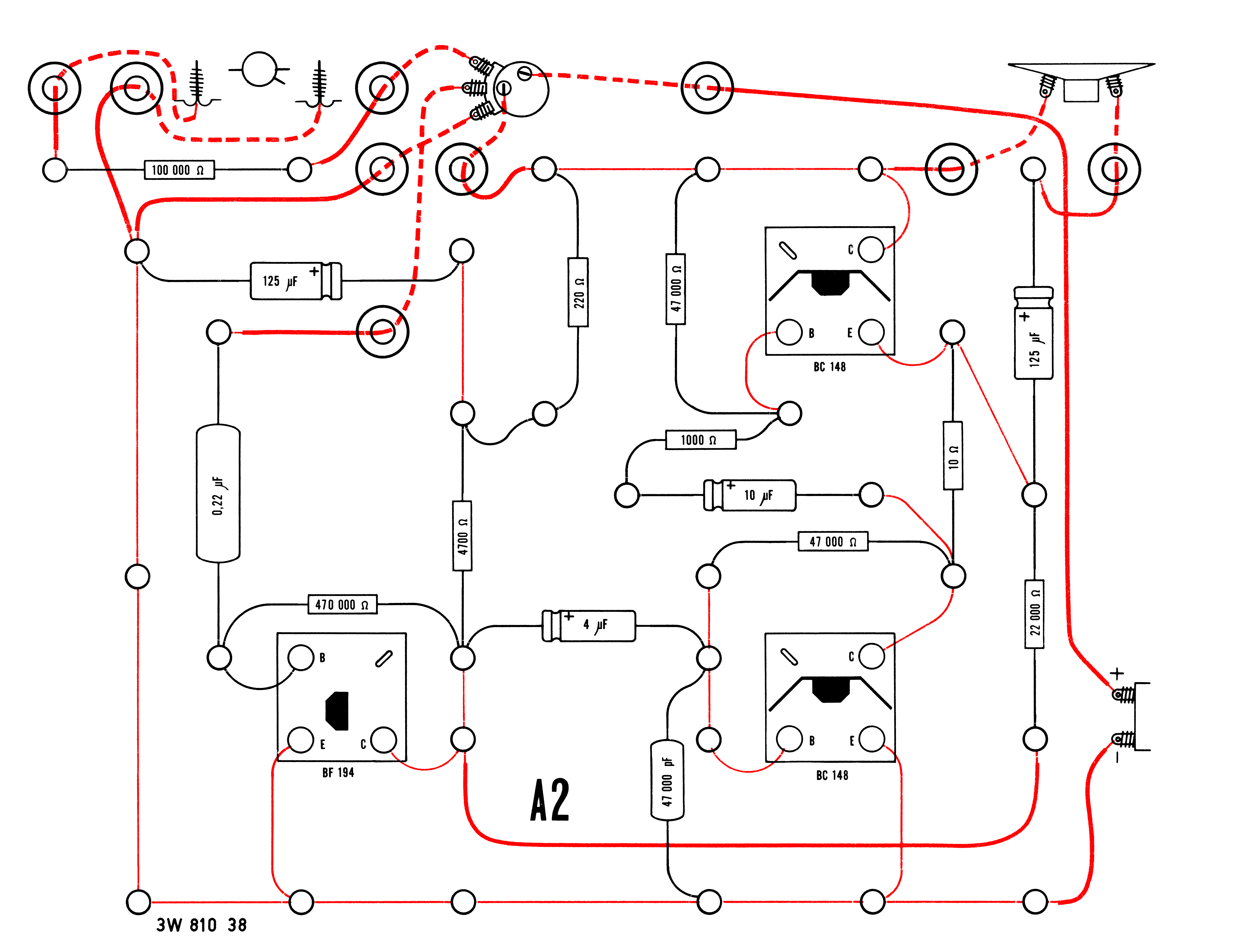
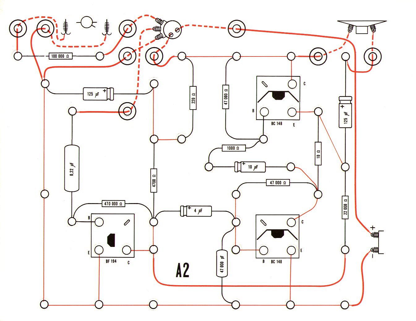
| A1 In version 2, the identifying number is missing, and the value of one of the capacitors is struck out for no apparent reason. | |||
|
|
|
|
|
|
|
|
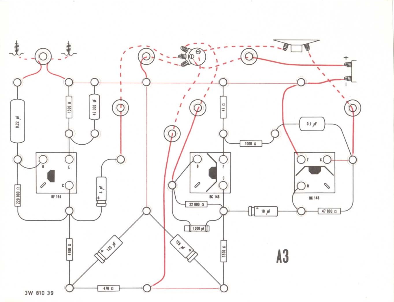
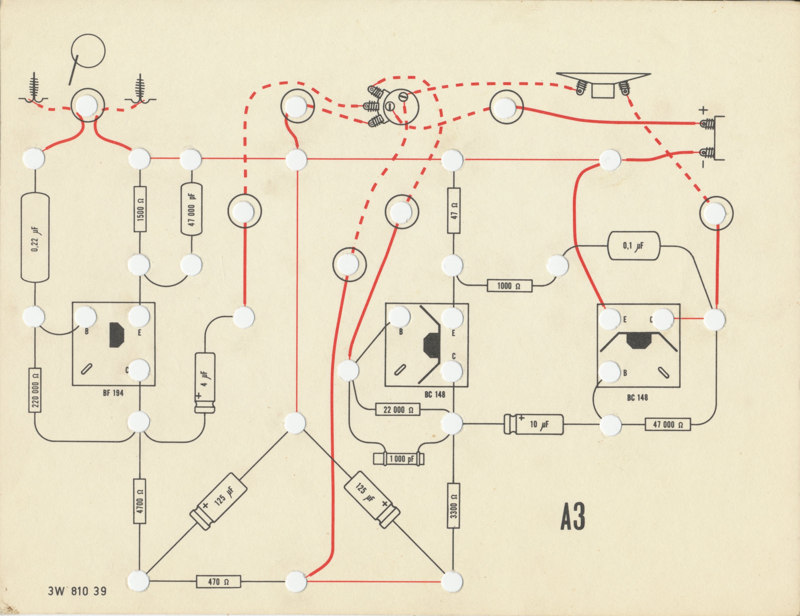
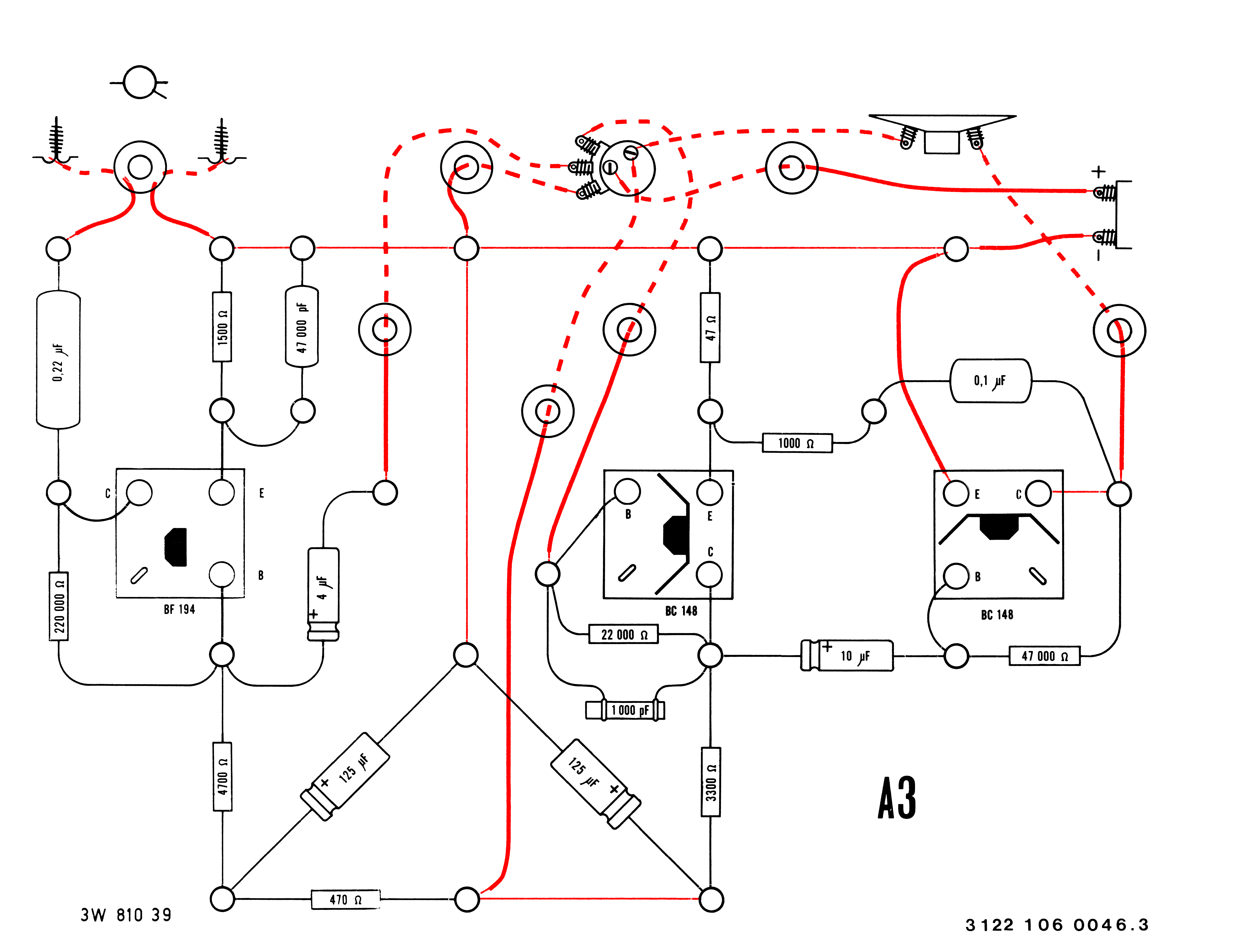
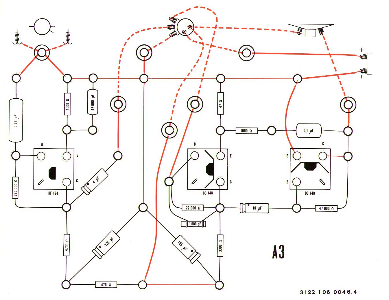
| A3 In version 2, the icon on the BF 194 transistor is incorrectly rotated 180° (but the connectors are still correctly labeled). In version 3, the icon is corrected, but now the connections are incorrectly labeled, swapping ‘B’ and ‘C’. Versions 1 and 4 are both correct. | |||
|
|
|
|
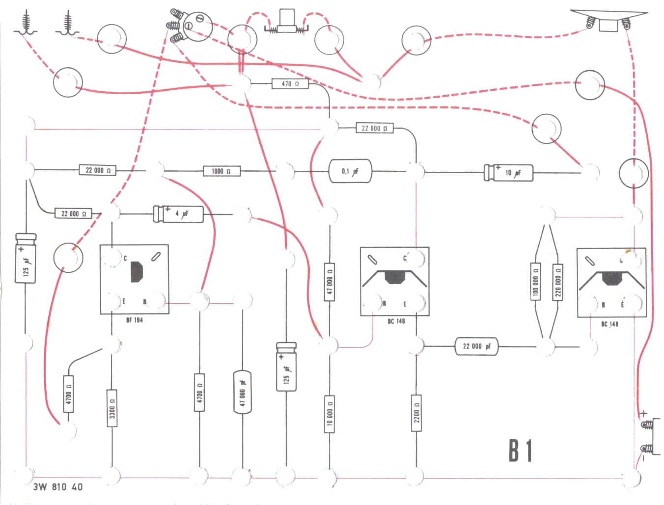
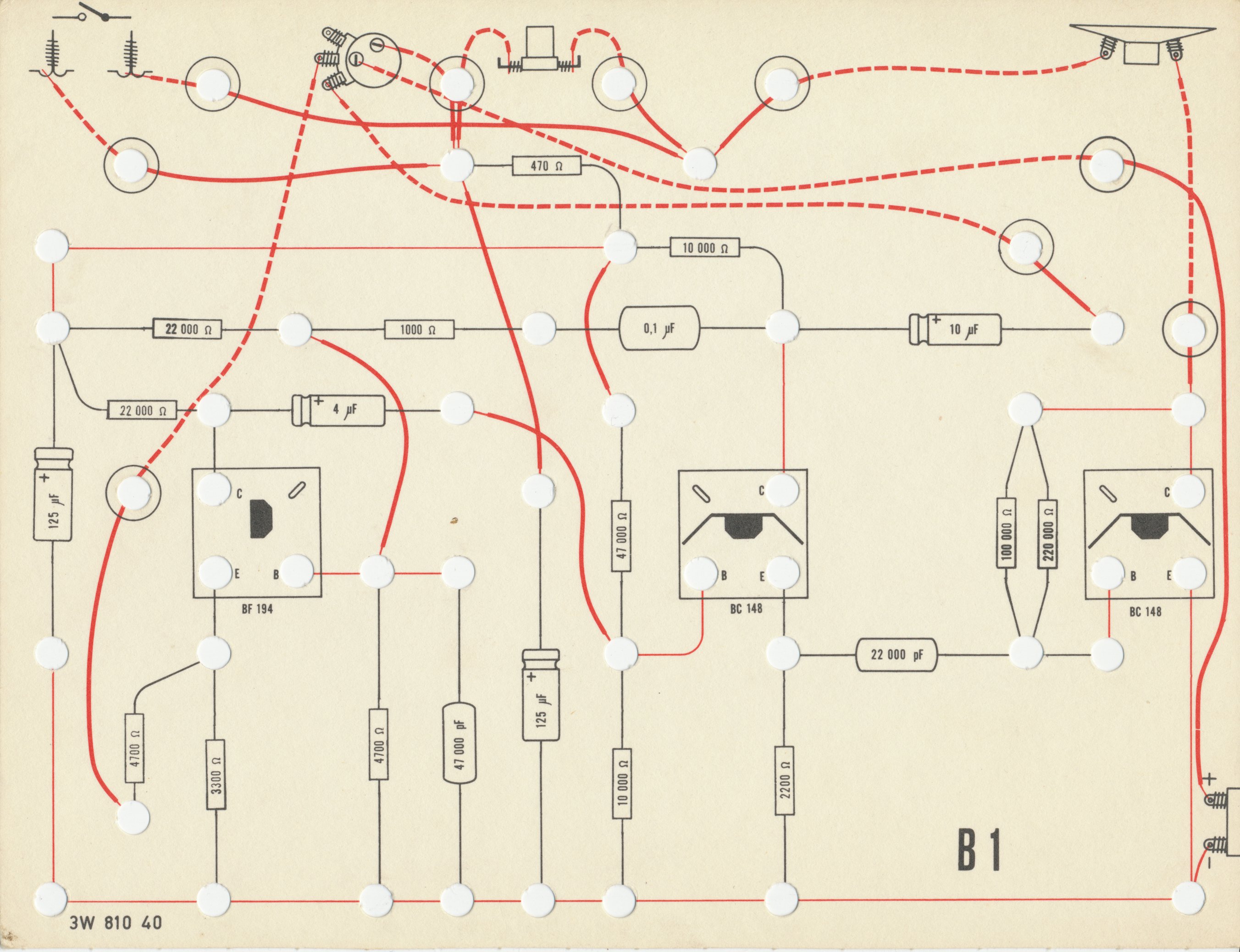
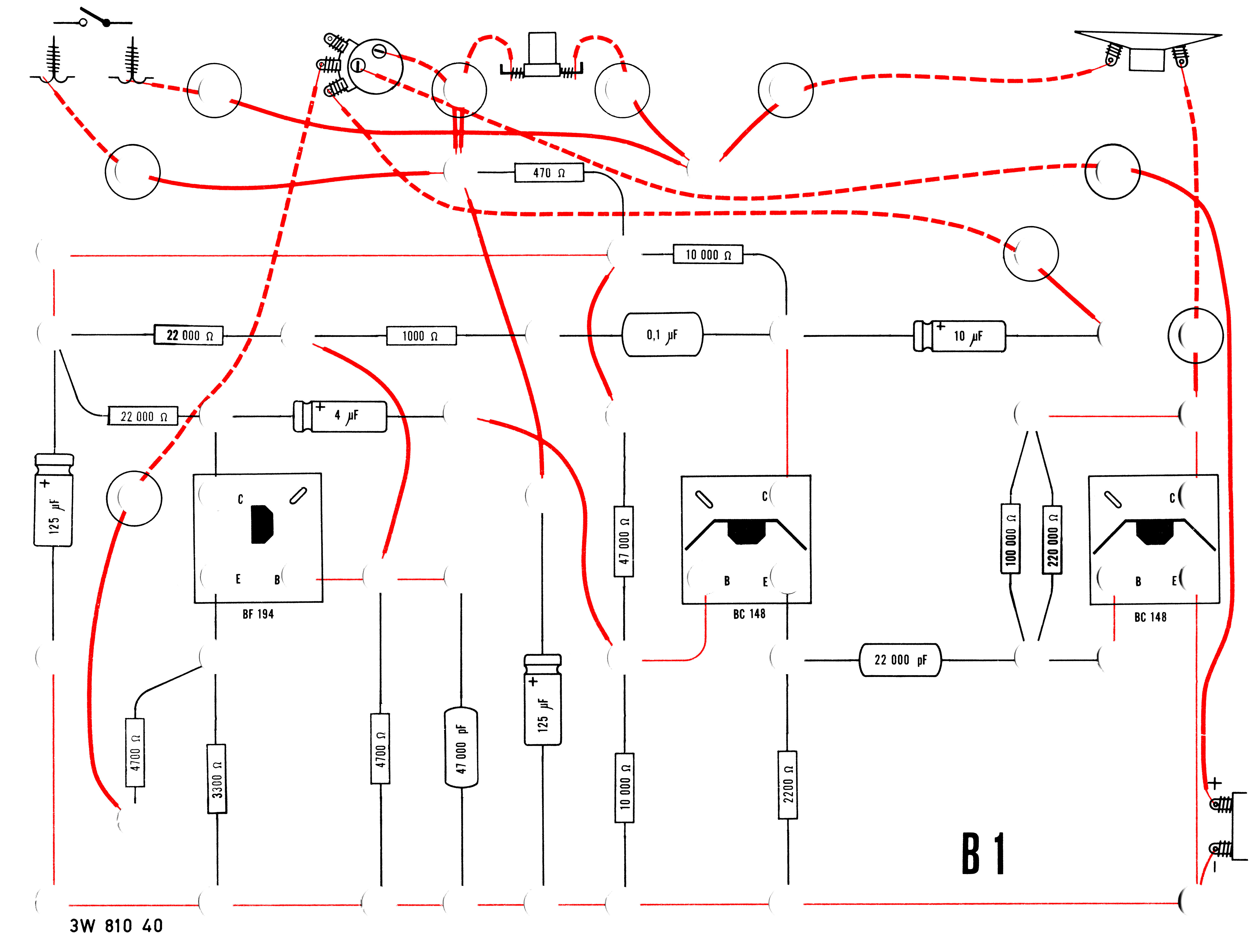
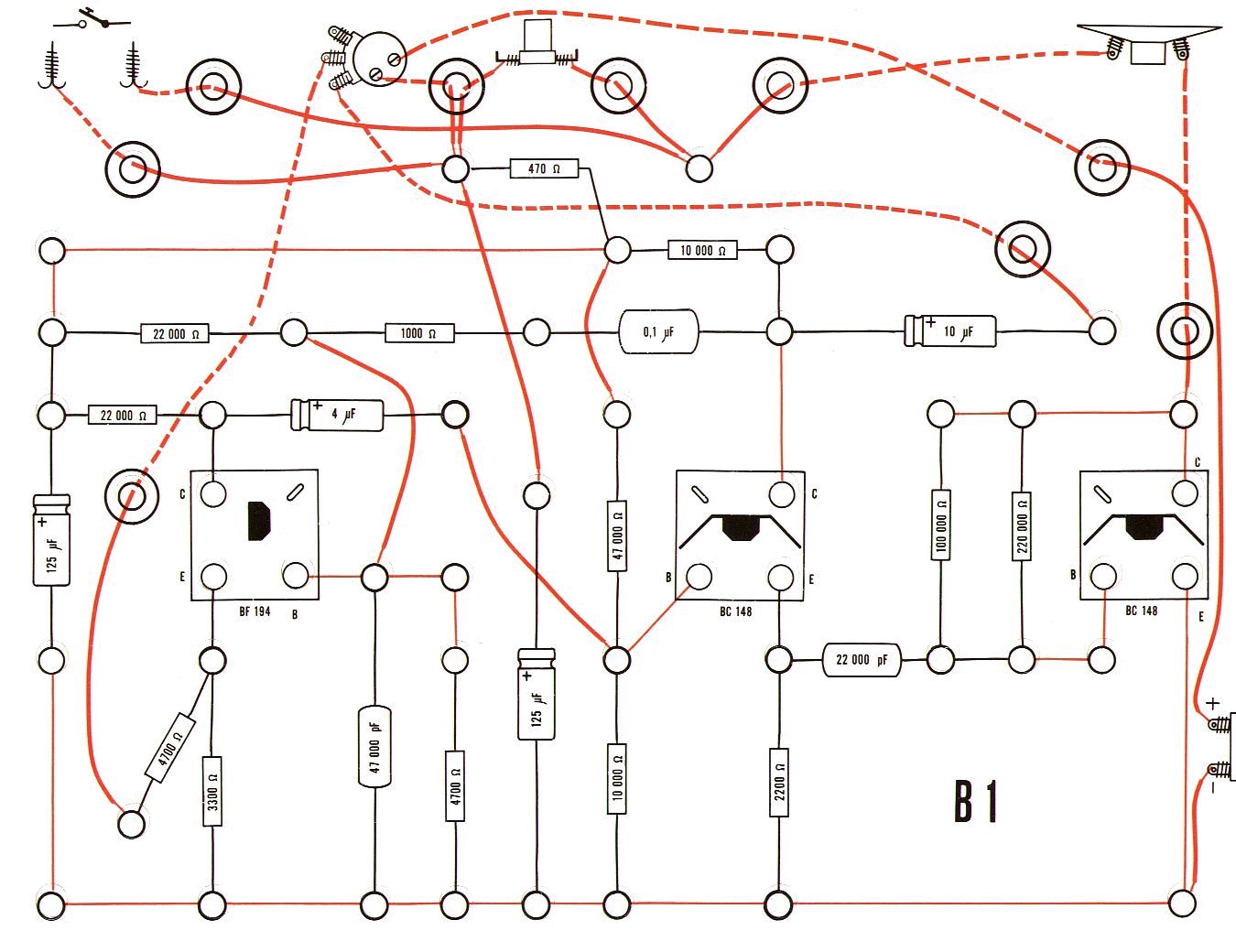
| B1 Version 1 has a wrong resistor value (22 000 Ω instead of 10 000 Ω). | |||
|
|
|
|
|
|
|
|
|
|
|
|
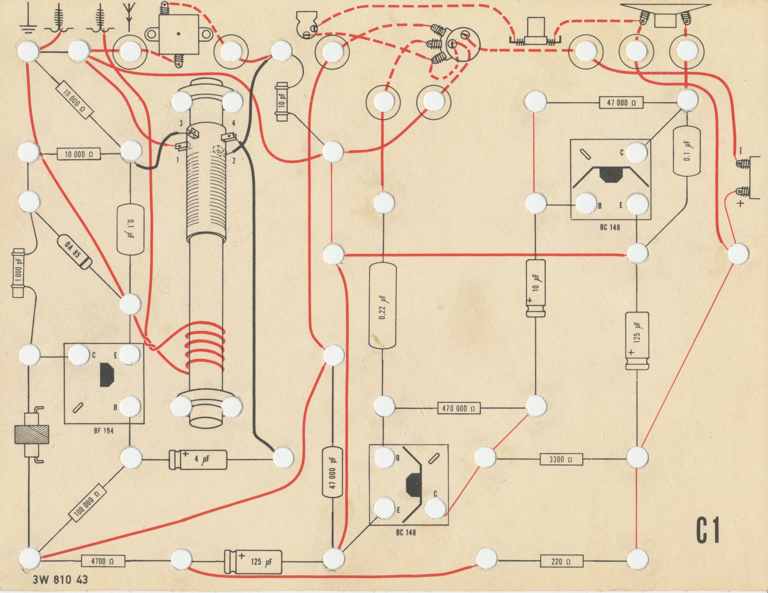
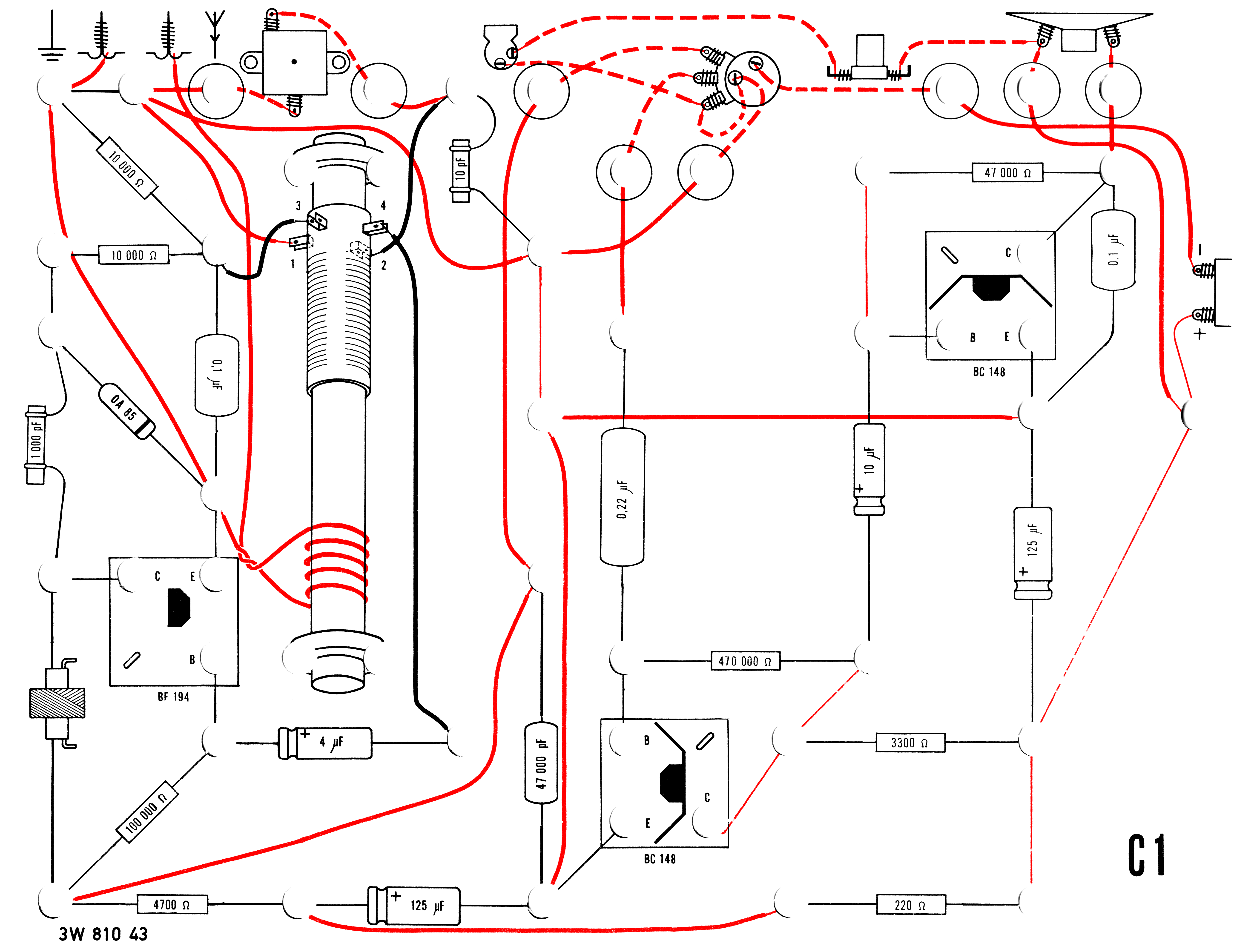
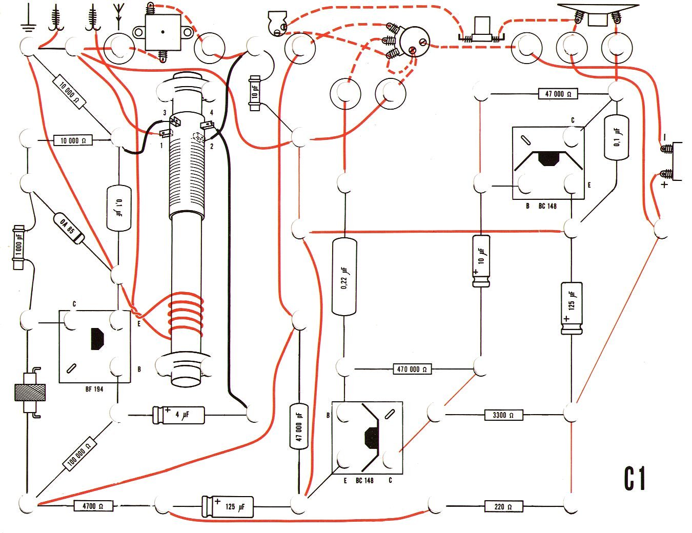
| C1 This diagram is missing from the set of version 1 scans, so a reconstruction is given here. | |||
|
|
|
|
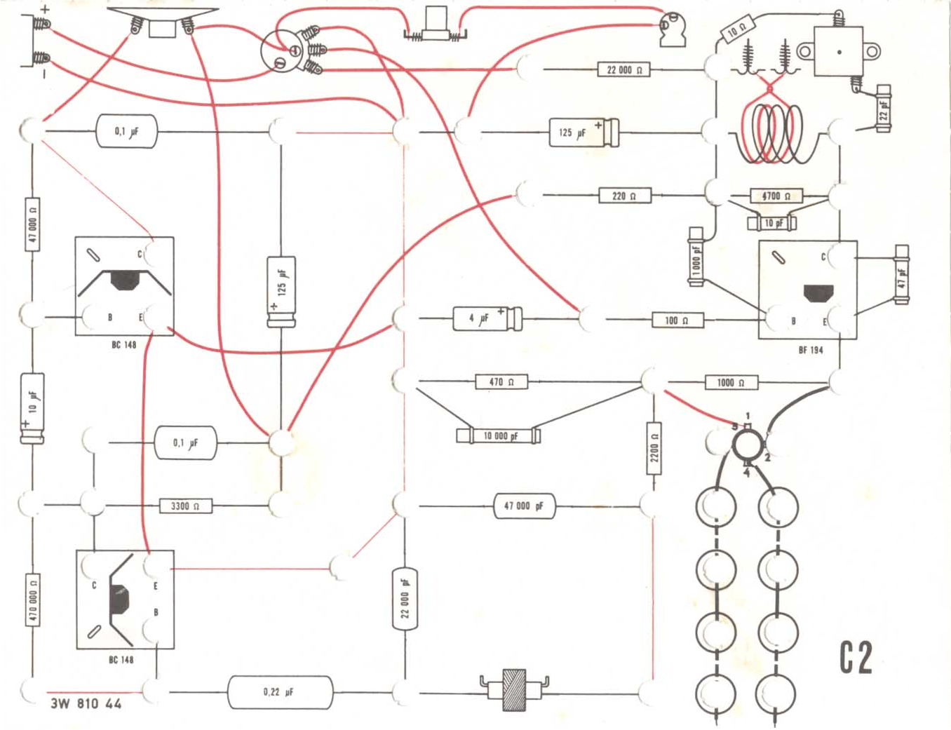
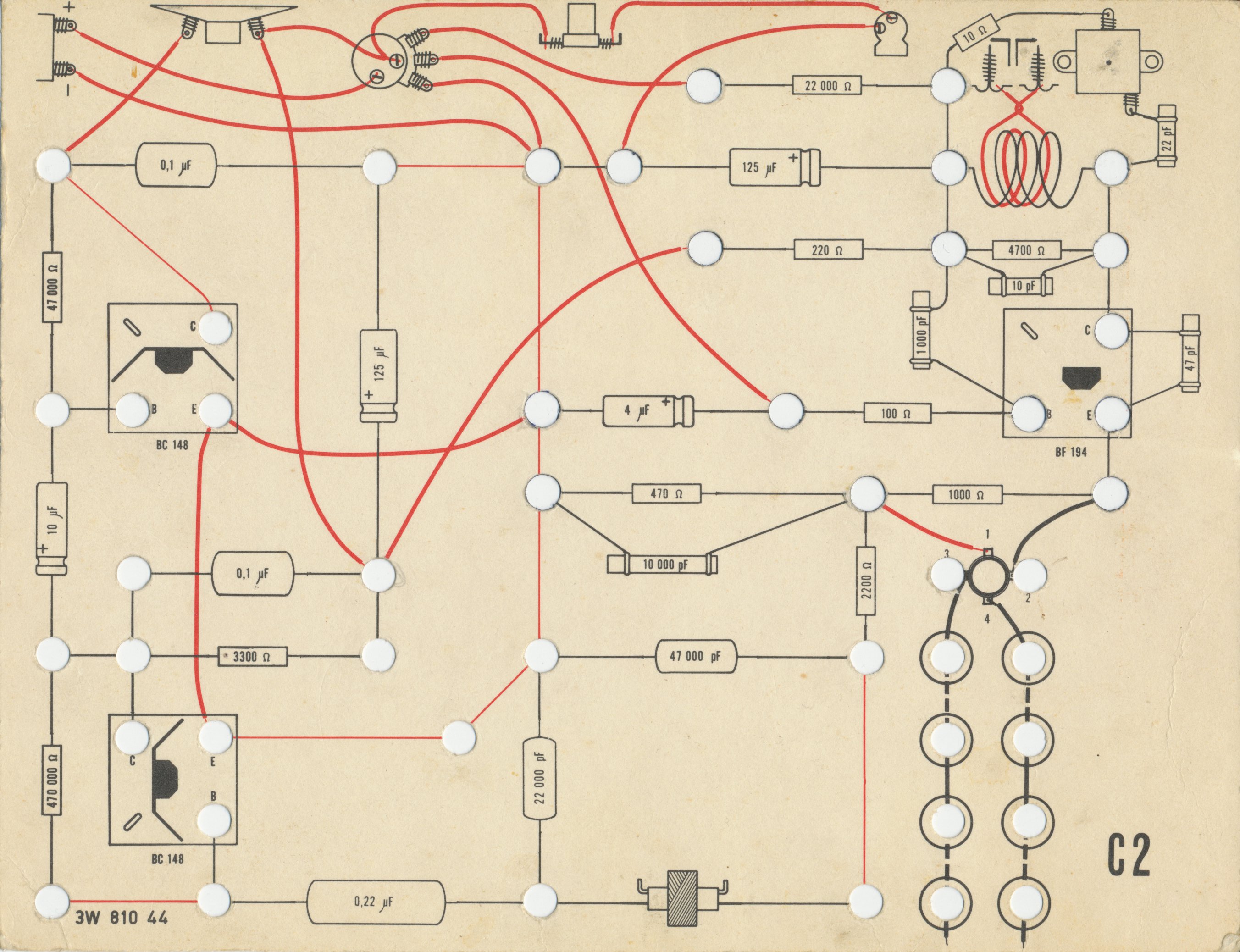
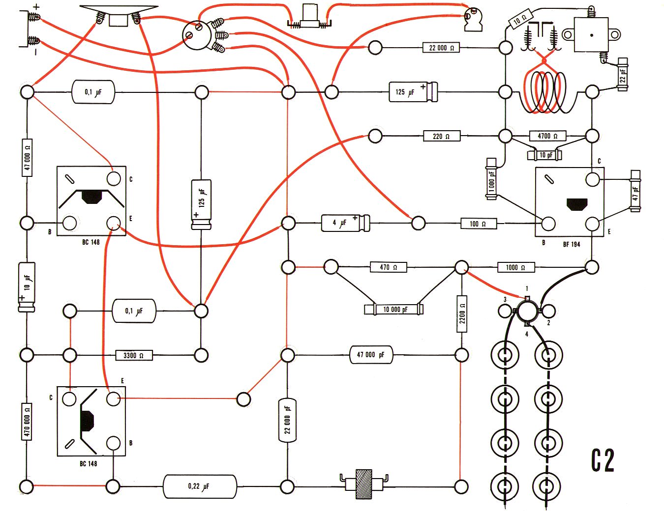
| C2 Version 1 has the potentiometer leads in the wrong order. | |||
|
|
|
|
|
|
|
|
|
|
|
|
|
|
|
|
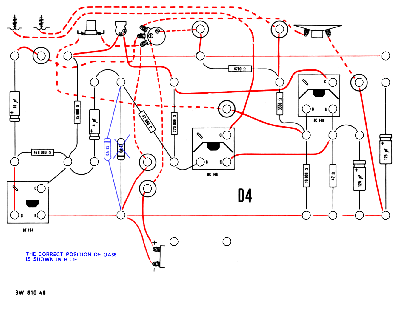
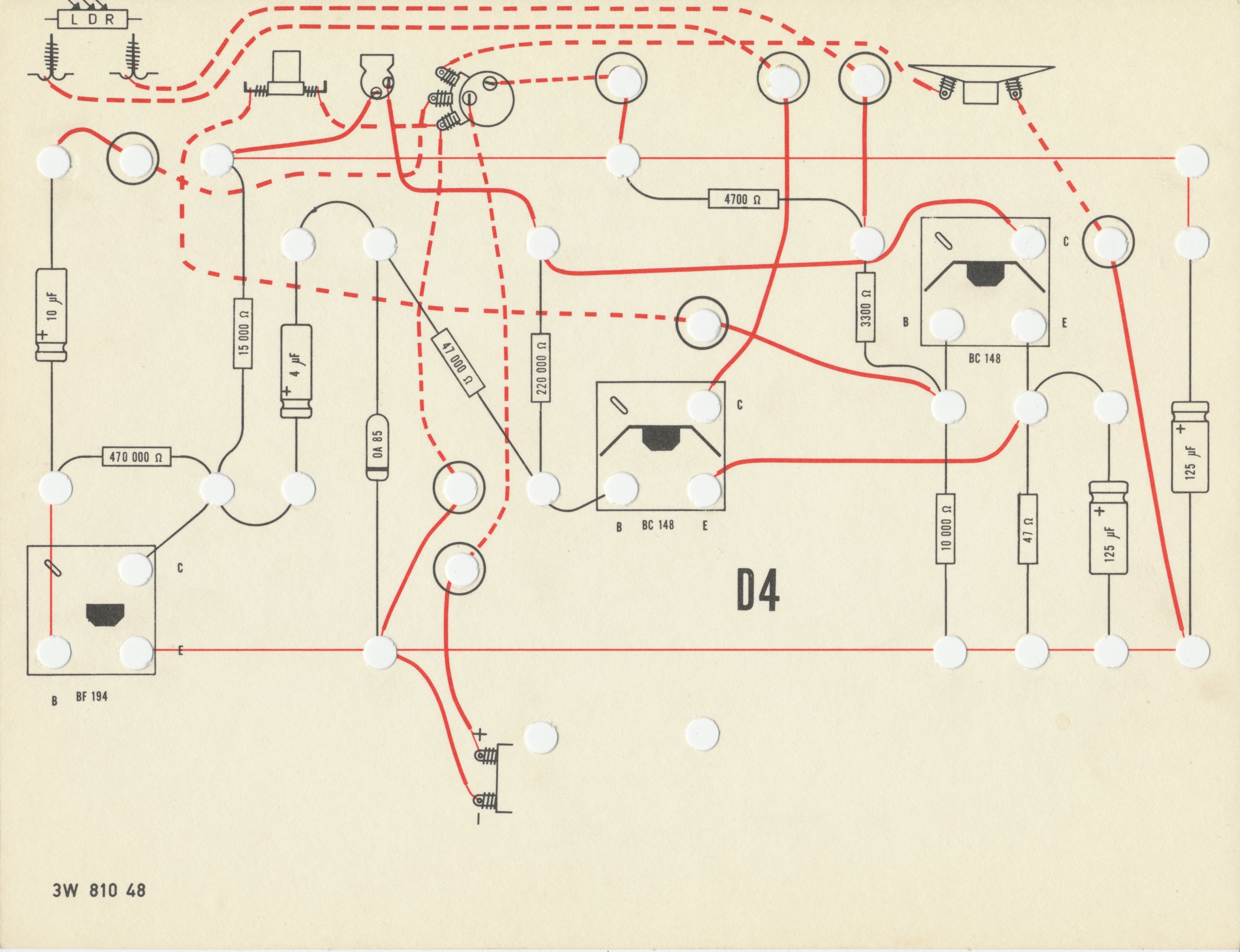
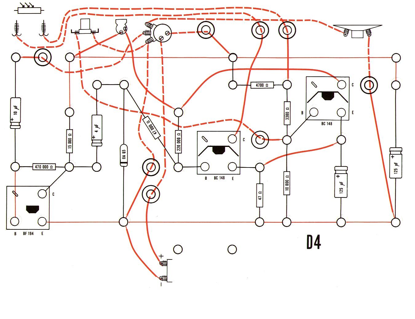
| D4 Version 1 surprisingly crosses out the diode and adds one in the opposite orientation in blue ink; however, the original orientation in the correct one and is retained in the later versions. | |||
|
|
|
|
|
|
|
|
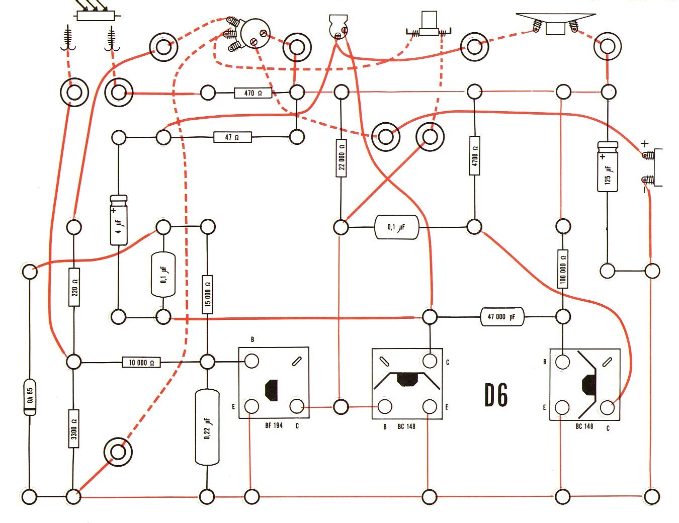
| D6 Version 1 has the potentiometer leads in the wrong order. | |||
|
|
|
|
|
|
|
|
|
|
|
|
|
|
|
|
|
|
|
|
|
|
|
|
|
|
|
|
|
|
|
|
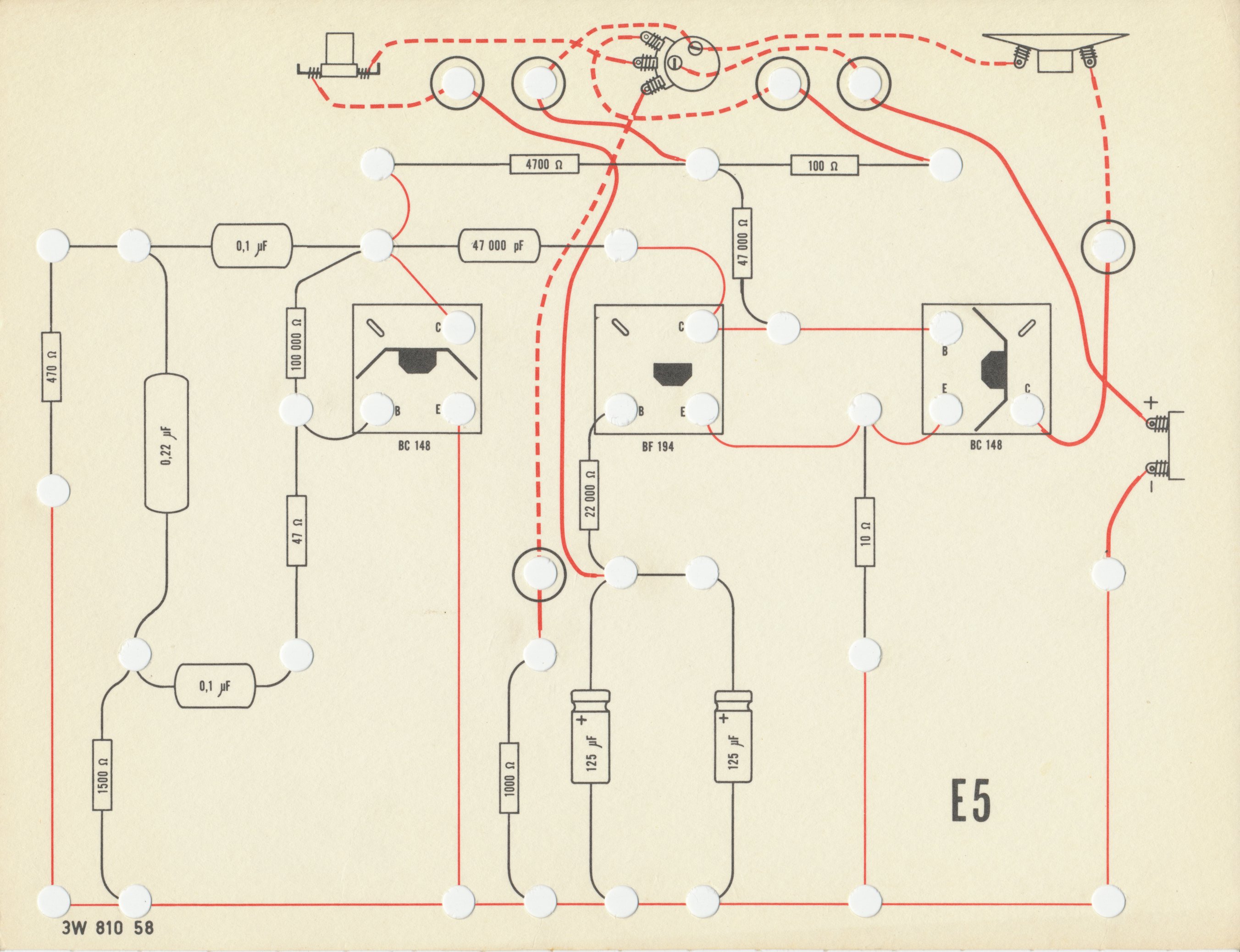
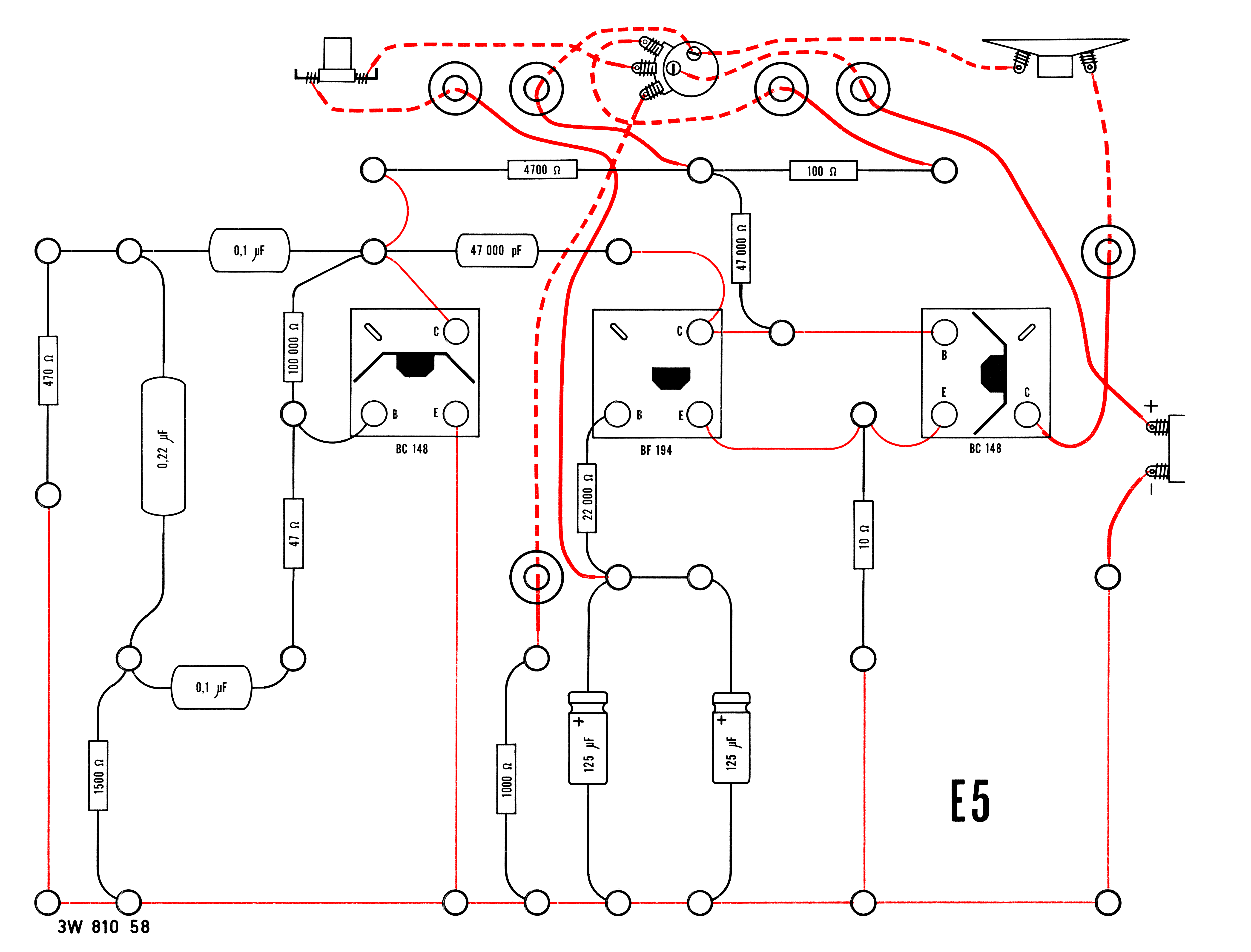
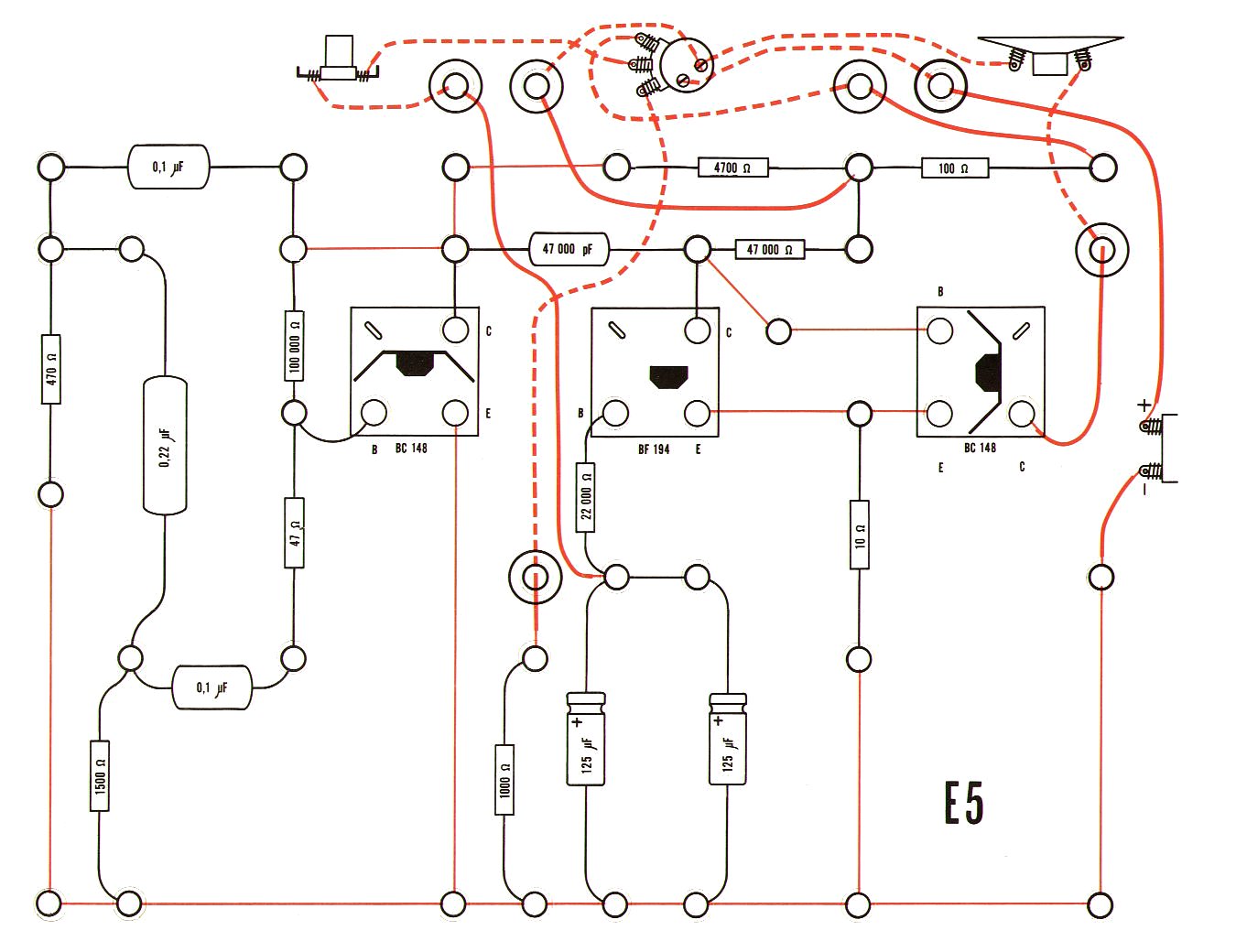
| E5 Version 1 has the potentiometer leads in the wrong order. | |||
|
|
|
|
|
|
|
|